
Dr.Abdul Kalam's view on Nanotechnology :
Gents,
In this post, I like to present Dr.Abdul kalam's view on Nanotechnology.
Here comes,
Nano Technology:
When I think of Nanoscience and Nanotechnology, I would like to discuss about three scientists who have laid the foundation on nanoscience and nanotechnology.
Mr. Richard Feynman, who described the concept of ‘building machines” atom by atom in his talk at Caltech titled “There is plenty of room at the bottom”.
Mr. Eric Drexler, who wrote the book titled ‘Nano Systems, Molecular machinery, manufacturing and computation”. Prof CNR Rao, who pioneered and fostered the nanoscience research in India.
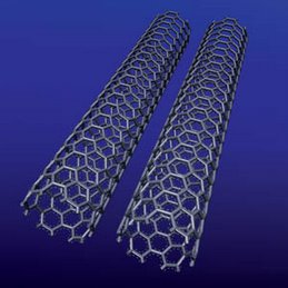
Molecular nano technology has enormous potential for future aerospace systems and health areas. Research has shown that newly discovered class of molecules, leading to the development of carbon nano tubes that they have multiple applications in the system developed in the areas of electronics particularly nano-electronics and power systems.
Carbon nano tubes are normal form of carbon with remarkable electrical and mechanical properties. It is hoped that such materials could revolutionize electronic design and open the space frontier by radically lowering the cost of launch to orbit.
Carbon Nano tubes reinforced with polymer matrix will result in composites which are super strong, light weight, small and intelligent structures in the field of material science. This has tremendous aerospace applications.
Molecular switches and circuits along with nano cell will pave the way for the next generation computers.
Ultra dense computer memory coupled with excellent electrical performance will result in low power, low cost, nano size and yet faster assemblies.
PRESIDENT’S ADDRESS AT THE INAUGURATION OF THE INDO-US NANOTECHNOLOGY CONCLAVE
Feb 22 2006 19:20 IST
Following is the text of the President, Dr. A.P.J. Abdul Kalam’s address at the inauguration of the Indo-US Nanotechnology Conclave:
Results of Nano Science and Technology Reaching the Societies
“Purposeful mission transcends limitations”
“I am indeed delighted to participate in the inauguration of Indo-US Nanotechnology Conclave organized by the Department of Science and Technology in partnership with Confederation of Indian Industry (CII) and Indo-US Science and Technology Forum.
I greet the organizers, scientists, technologists, industry captains, academia, venture capitalists and the distinguished invitees.
I am also very happy to see that a pioneer in nano science Prof. CNR Rao has given the key note address for this Indo-US conclave and I find that this Conclave is being organized with the participation of all the stakeholders from the researchers to the users of nano-technology.
This will definitely ensure integrated definition of the problem and enable the scientific community, technological community, academicians, industrialists and venture capitalists to work together and provide cost effective quality products using nano-technology to the global society at the right time.
Products progress in Nano Science & Technology in India – some examples
A. Water: Nano tube filter - water purification
The scientists from Banaras Hindu University have devised a simple method to produce carbon nanotube filters that efficiently remove micro-to nano-scale contaminants from water and heavy hydrocarbons from petroleum.
Made entirely of carbon nanotubes, the filters are easily manufactured using a novel method for controlling the cylindrical geometry of the structure. The work was supported in part by the Ministry of Human Resource Development and Department of Science and Technology in India
The filters are hollow carbon cylinders several centimeters long and one or two centimeters wide with walls just one-third to one-half a millimeter thick. They are produced by spraying benzene into a tube-shaped quartz mold and heating the mold to 900°C. The nanotube composition makes the filters strong, reusable, and heat resistant, and they can be cleaned easily for reuse.
The carbon nanotube filters offer a level of precision suitable for different applications. They can remove 25-nanometer-sized polio viruses from water, as well as larger pathogens, such as E. coli and Staphylococcus aurous bacteria.
The researchers believe this could make the filters adaptable to micro fluidics applications that separate chemicals in drug discovery. This is a classic application of the latest in science – Nano science, to age old problem of water purification.
If properly used, this can help in lessoning the burden in our drinking water missions leading to the availability of safe drinking water that will result in minimizing the water borne diseases.
B. Healthcare:
Typhoid Detection Kit Typhoid Detection Kit has been developed by DRDE, Gwalior using the nano sensor developed by Prof. A.K. Sood, and his team from IISc, Bangalore.
Typhoid fever caused by Salmonella typhi is a major health problem and an important challenge to health authorities of third world countries due to unsatisfactory water supply, poor sanitary conditions, malnutrition, emergence of antibiotic resistant strains etc.
According to an estimate the worldwide incidence to typhoid fever is 16 million cases annually and death rate is 6 lakhs individual per year worldwide.
In India, the morbidity due to typhoid varies from 102 to 2219/100,000 population in different parts of the countries. In some areas typhoid fever is responsible for 2-5% of all deaths.
In India for routine diagnosis for typhoid disease Widal test is performed with single serum sample which does not provide the correct diagnosis of infection. Therefore a Latex agglutination based test has been developed at DRDE, Gwalior using recombinant DNA technology and immunological technique for rapid diagnosis of typhoid infection.
The test detects S. typhi antigen directly in patient’s serum within 1-3 minutes which is very important for initiating early treatment and saving human life.
A collaborative work has been carried out with Prof. A.K. Sood of Indian Institute of Science, Bangalore, the sensitivity of the test has been increased 30 times by applying a small electric charge (1.5 V).
With this improvement, extreme low concentrations of the antigen in clinical sample can be detected. Moreover, very small quantity of clinical sample as low as 2-3 µl is required to perform the above test as compared to 10-15 µl sample required for latex agglutination test.
C. Power:
Gas flow induced generation of voltage from solids Prof AK Sood, professor of Physics at IISc and his student Shankar Ghosh has studied, experimented and found that the liquid flow in carbon nano tubes can generate electric current.
One of the most exciting applications to emerge from the discovery is the possibility of a heart pacemaker – like device with nanotubes, which will sit in the human body and generate power from blood.
Instead of batteries, the device will generate power by itself to regulate defective heart rhythm. The IISc has transferred the exclusive rights of the technology to an American start-up Trident Metrologies.
They will develop the prototypes and commercialize the gas flow sensors.
D. Drug delivery system
A research group headed by Professor A. N. Maitra of the University of Delhi’s Chemistry Department has developed 11 patentable technologies for improved drug delivery systems using nanoparticles.
Four of these processes have been granted U.S. patents. One of the important achievements at the initial stage of drug delivery research was development of a reverse micelles based process for the synthesis of hydrogel and 'smart' hydrogel nanoparticles for encapsulating water-soluble drugs.
This method enabled one to synthesize hydrogel nanoparticles of size less than 100nm diameter. This technology has been sold to Dabur Research Foundation in 1999. Another technology has been transferred to industry deals with nanoparticle drug delivery for eye diseases.
Traditionally, steroids have been used extensively in the treatment of ocular inflammatory disease and allergies.
However, prolonged use of steroids has many side effects. The Delhi university group’s process uses nanoparticles to encapsulate non-steroidal drugs.
"This process improves the bioavailability of the drug on the surface of the cornea".
The technology has been transferred to Chandigarh-based Panacea Biotech Ltd.
E. Microwave
CNTs Production unit DMSRDE, Kanpur is synthesizing non-aligned, quasi-aligned and aligned CNT with a batch size of 50 grams using a fast synthesis process.
It has a maximum operating temperature 12000 C. The CNTs will have applications in EM absorbers, composites, gas sensors, flow monitors, field emission devices.
Nano technology product survey:
There may be many more achievements in our scientific laboratories; I suggest DST and CII to jointly conduct a survey to prepare the technological breakthroughs accomplished in nano technology products in India.
Now let me discuss, what I have witnessed on the convergence of technologies in Bio-Nano and Info in Singapore and Republic of Korea.
Nano science & Technology Focused research in East Asia
During my recent visit to Singapore, I visited the facility built up in Biopolis, Singapore. There I saw an innovative programme of development of quality manpower in life sciences.
Biopolis has a scheme of searching talent globally and providing them all the facilities to acquire qualification of their choice from any University located in the world.
They provide the funds for the entire programme of study and they require the students to come back and work in Singapore in the field of life sciences for a minimum of six years.
This idea has emanated because they want quality manpower across the world to enhance their R&D potential leading to commercialization initiatives.
I am sure; there is an important message for all of us for nurturing young talent for all scientific research work particularly in nano-science and nano-technology.
We have 540 million youth in the country, we have to build the capacity among the aspiring youth at the graduate, post graduate and Ph.D level. Ministry of Human Resource Development and DST have to launch a major capacity building drive for developing the human resource on convergence of technologies in the Bio, Info and Nano science and technologies.
Nano cluster:
Nanyang Technological University has created a Nano science and Nano Technology cluster, which is a NTU wide network of research center with shared facilities for Nano fabrication, Nano characterization and exploitation of Nano technology applications.
Focused areas of research, development and commercialization include
Nano devices,
Energy & Catalysis,
Nano Magnetics & Photonics,
Organic Molecular Electronics,
Nano – Biotech and Nano Materials: Synthesis.
I visited the Nano Cluster labs and witnessed the developed products such as:
a. Electronic Biochips:
Microfluidic protein biochip for electrochemical immunoassays with dual ring electrode.
b. Development of PLZT (Lanthanum-substituted lead zirconate titanate) electro-optical ceramics for eye-protection devices: It can rotate the plane of incident light polarization from 00 to 900 by electric-induced birefringence.
So, PLZT ceramics can be applied in eye protection devices, protecting eyes or optical sensors from suddenly incident intense light. It provides low driving voltage and fast response time.
c. Field emission x-ray source:
Development of compact x-ray source based on CNTs (Carbon Nano Tubes) and carbon nano fibers as an electron emitter for 3-D inspection and biomedical applications.
Nano Fab:
I had visited the Samsung Electronics, Giheung Plant in Korea during my recent visit to Republic of Korea. They are the leaders in semiconductor, tele-communication, digital media and digital convergence technologies.
Out of the eight new fabrication lines, Samsung is designing four with capacities higher than conventional lines with the possibility of a 300 mm or lager wafer-unit, it includes one R&D line.
This has resulted in a steep growth in global memory semiconductor market share for Samsung on a year to year basis. Also, I had a glimpse of the nano technology research in Samsung.
Using this technology and the bioinformatics the researchers in Samsung are developing a chip that can be used to diagnose common diseases even at home.
Once the patient knows reasonably well the problem, will use the information to chose the doctor, the treatment options, and possible outcome
This visit has given me an insight, about how they plan and execute right from science, research, technology development, product development and commercialization aiming at positioning the products in the world market within a specified time frame.
I have witnessed that the integrated planning includes capacity building, establishment of centers of excellence, creation of world class infrastructure, transfer of technologies to industrial partners and marketing.
A way ahead
I have studied India’s scientific and technological work after independence. There have been some excellent areas of basic research in very advanced topic right from late 1950s and 60s.
For example we had excellent work on aero science, material science and also excellent work on semi-conductor research. Some world class scientists published papers also.
Later even in the Liquid Crystal Display (LCD) area some original work was done by Raman Research Institute. We should now work to realize world class materials.
However, when one studies the technological and commercial aspects of these areas, the results have not been commensurate. We never produced an indigenous aircraft until very recently.
Also we missed micro electronic revolution in the 70s.
Similarly, in Liquid Crystal Display, we never even started a good commercial production whereas countries like Taiwan and South Korea have become world leaders in commercial production of these products.
If we study, many areas, such trend seems to be the pattern.
We should not repeat this again in areas like Nano-Technology and Convergence of nano-technology with ICT and BT.
Therefore, even while we are concentrating on basic research with eminent scientists working in it, simultaneously Indian industrial group small, big and medium should concurrently work on commercialization of nano-technologies.
It may well be that the technologies are developed in India or in USA or in other countries. The main focus should be speedy commercialization to fit into the global market.
The time is now ripe since our economy is in the ascent phase and the manufacturing sector has established adequate capacity to promote rapid commercialization of products.
Towards this, I suggest that separate funds which can be used primarily for commercialization by Indian industry either for in-house or partnership mode for specific product should be encouraged at the earliest.
And innovative managerial mechanism has to be there to utilize these funds with utmost speed and with commercial success in mind. The project should be market driven. I would suggest to the government to set apart sufficient funds on non-lapsable basis for nano-technology commercialization, and I would like industries to take a lead in this matter.
Simultaneously, there is a need to take action to build the human resource required for undertaking the challenging tasks in this new sector.
I would recommend the nano-technology community, particularly, the industrialists to read the book titled "Nano-Technology Market and Company Report" - finding hidden pearls prepared by Deutsche Bank and other experts, with details of over 350 nanocompanies and interviews with over 100 entrepreneurs.
We should mount a mission mode operation to deliver tangible products to meet our national demand as well as to be beneficial to the other countries. Let me discuss some of the national missions and the possible areas of research, design, development and production of products with reference to the areas of importance for development using nano science and technologies.
Agriculture and food processing:
We are in the mission of generating 400 tones of food grains with reduced land, with reduced water and with reduced workforce. It is essential to take an agro food processing in a big way which will bring employment potential in rural areas. Some of the possible areas of research in agriculture and food processing are:
Nano-porous zeo-lites for slow-release and efficient doses of water and fertilizers for plant, and of nutrients and drugs for livestock, nano-capsules for herbicide delivery, nano sensors for soil quality and for plant health monitoring.
Nano-composites for plastic film coatings used in food packaging, antimicrobial nano-emulsions for applications in decontamination of food equipment, packaging or food processing are other important areas of research.
Infrastructure:
India is aspiring to build hundred million homes within next ten years.
The infrastructure development in metropolitan and tier-2 cities needs to be enhanced in the form of new bridges, airports, marketing complexes and industrial units. 40% of the rural areas need to be covered with all weather roads; we need to double the present national highways ratio for the 100 square kilometer area.
Can nano-science material and technology research provide a solution? Our research focus in the nano-material should be towards cheaper rural housing, surfaces, coatings, use of concrete with heat and light exclusion;
Can we develop heat resistance nano-material to block ultraviolet and infra red radiation;
Can we develop a nano-molecular structure to make concrete more robust to water seepage,
Can we have self cleaning surfaces with bio active coating?
Energy:
Energy Independence has to be our nation's first and highest priority. We must be determined to achieve this within the next 25 years i.e by the year 2030.
When our population may touch 1.4 billion people, demand from power sector will increase from the existing 120,000 MW to about 400,000 MW.
This assumes an energy growth rate of 5% per annum. Electric power generation in India now accesses four basic energy sources:
Fossil fuels such as oil, natural gas and coal; Hydroelectricity; Nuclear power; and Renewable energy sources such as bio-fuels, solar, biomass, wind and ocean. Fortunately for us, 89% of energy used for power generation today is indigenous, from coal (56%), hydroelectricity (25%), nuclear power (3%) and Renewable (5%). Solar energy segment contributes just 0.2% of our energy production.
Thus it would be seen that only 11% of electric power generation is dependent on oil and natural gas which is mostly imported at enormous cost. Only 1% of oil is (about 2-3 million tonnes of oil) being used every year for producing electricity.
However, power generation to the extent of 10% is dependent on high cost gas supplies. The most significant aspect, however would be that the power generated through renewable energy technologies may target 20 to 25% against the present 5%.
Keeping this requirement in mind, can we find an innovative solution for the use of nano-technology using higher efficiency CNT based solar photovoltaic cells with an efficiency of 45% in partnership with Penn State University? This will enable setting up of modular hundred megawatts solar SPV plants across the country in a reduced land with reduced cost when compared to present figure of Rs. 20 Crore per megawatt SPV plant with 14% efficiency photovoltaic cells. Can we also develop novel hydrogen storage systems based on carbon nano tube for energy storage?
Safe Drinking Water:
Over 50% people do not have safe drinking water in India. Shall we embark on a mission for water purification, water de-toxification, water desalination through nano membranes and nano sensor for detecting contaminants and pathogens? How the nano-porous zeo-lites, nano-porous polymers can be used to design and develop products for water purification.
Healthcare:
India has already patented the development of drug delivery system using nano-technology. Stem cell research in India is advancing in the field of cardiology, ophthalmology, diabetic research, endocrinology, oncology and immunology. It is essential to develop drug delivery system for stem cell implantation into the specific organs of the body related to the ailment using nano technology.
Aero Space:
Emerging technologies such as MEMS, Nano, Information technology, biotechnology, space research, Hypersonic, High power lasers and microwave will be dominating the future in every field and applications. The advancements in material science and technology will give a major thrust to the realization of advanced aerospace systems.
We are today at the convergence of Nano, Bio and Information technologies, that will lead to new generation aero space devices and products.
Molecular nano technology has enormous potential for future aerospace systems. Research has shown that newly discovered class of molecules, particularly carbon nano tubes built from graphite sheets curved into a wide variety of close shapes, may lead to tougher, high temperature materials that can survive in vacuum and other harsh environments.
Carbon nano tubes are normal form of carbon with remarkable electrical and mechanical properties. It is hoped that such materials could revolutionize electronic design and open the space frontier by radically lowering the cost of launch to orbit.
Carbon Nano Tubes reinforced with polymer matrix will result in compo-sites which are super strong, light weight, small and intelligent structures in the field of material science. This has tremendous aerospace applications.
ICT:
Molecular switches and circuits along with nano cell will pave the way for the next generation computers. Ultra dense computer memory coupled with excellent electrical performance will result in low power, low cost, nano size and yet faster assemblies. This will result in the small scale assembly of computers, tablet PCs, display systems etc., With the emergence of Nanotechnology, there is convergence of nano-bio-info technologies resulting new devices which has wider applications in structure, electronics, and healthcare and space systems.
Potential applications are virtually endless. Progress in nanotechnology is spurred by collaboration among researchers in material science, mechanical engineering, computer science, molecular biology, physics, electrical engineering, chemistry, medicine and aerospace engineering.
This is one of the important emerging area which brings synergy in research and development by combining the strengths of the multiple domain knowledge leading to the creation of knowledge society.
Our educational institutions and universities should have a special purpose missions based on their core competence.
Nano Science and Technology Consortium (NASTCON)
I am confident that the Indian nano technology initiatives are maturing into marketable products for worldwide applications. Industries from abroad and India are keen to take our technologies and to commercialize.
Indian industries now should take the lead and become a partner in the nano science and technology ventures to capture the international market.
Next ten years will see nano technology playing the most dominant role in the global business environment and is expected to go beyond the billion dollar estimates and cross the figure of $ ONE trillion.
The market share for the nano technology products such as Nano materials will be about $ 340 billion, Electronics and Semi conductors will be $300 billion, Pharmaceutical will be around $ 180 billion and Aerospace and chemical plants and tools will be around $ 200 billion.
In this scenario, it is essential to have a focussed mission to capture at least 5% ($50 billion) market share within 10 years time from now, using our core competence with international partnership.
We have to launch vertical missions under an umbrella organisation (like CII/NASSCOM) with the public-private investment in at least 10 nano technology products in Water, Energy,
Agriculture, Healthcare, Space and Defence and ICT sectors. In these identified vertical missions DST, R&D institutions, Universities, Indian Private Industries, CII, FICCI and NASSCOM should work together in partnership with international industry and academia partners for faster design, development and production of products for world market.
Conclusion
In order to achieve this mission, we need to connect all the relevant institutions participating in this mission using the high bandwidth fiber optics network into a Knowledge Grid specially established for the nano technology mission of India and partnering nations. Recently, I have proposed the establishment of "World Knowledge Platform" which will combine the core competence of the partners in the area of convergence of technologies in Bio-Info-Nano technologies for the design, development and product realization.
Do not get into soft research in the international co-operation. You must go for applied research. Nations should work towards a win-win situation in product development and international marketing.
I recall the great saying of the Saint Maharishi Pathanjali in Yoga Sutra at 500 BC:
’When you are inspired by some great purpose, some extraordinary project, all your thoughts break their bounds, your mind transcends limitations, your consciousness expands in every direction, and you find yourself in a new, great and wonderful world. Dormant forces, faculties and talents come alive, and you discover yourself to be a greater person by far than you ever dreamt yourself to be.’
Hence, I request the scientific, research, industrial and business community assembled from India and US and other participants to embark on a goal oriented research, development and commercialization missions on nano science and technologies for societal applications.
Encourage the youth to take up the challenge in these missions with international collaborations.
I inaugurate the Indo-US nano technology conclave and wish the Conference all success.
May God Bless you.”
Source : Press Information Bureau. Government of India


